


FE-SEM is an advanced electron microscopy technique that utilizes a focused beam of electrons to scan the surface of a sample, generating high-resolution images and providing valuable information about its topography, morphology, and elemental composition. Unlike conventional SEMs that use thermionic electron sources, FE-SEMs employ a field emission gun (FEG), which produces a much brighter and narrower electron beam. This results in significantly improved spatial resolution (down to 1-2 nm), clearer images with less electrostatic distortion, and the ability to image sensitive or non-conductive materials at lower accelerating voltages. FE-SEM finds extensive applications in various fields, including materials science, nanotechnology, semiconductor research, and biological sciences, for analyzing structures ranging from nanoparticles and thin films to biological specimens and microchips.
Energy Dispersive X-ray Spectroscopy (EDS or EDX) is an analytical technique often associated with SEM used for the elemental analysis and chemical characterization of materials. An EDS detector measures the energy and intensity of the X-rays emitted by electron bombardment on the sample, generating a spectrum that plots X-ray counts against energy. By identifying the characteristic energy peaks in the spectrum, the elemental composition of the sample can be determined qualitatively, and the intensity of these peaks can be used for quantitative analysis, revealing the relative abundance of each element. This technique is invaluable across diverse fields such as materials science, nanotechnology, and forensics, providing crucial information on elemental distribution and identification, even at the micro and nanoscale
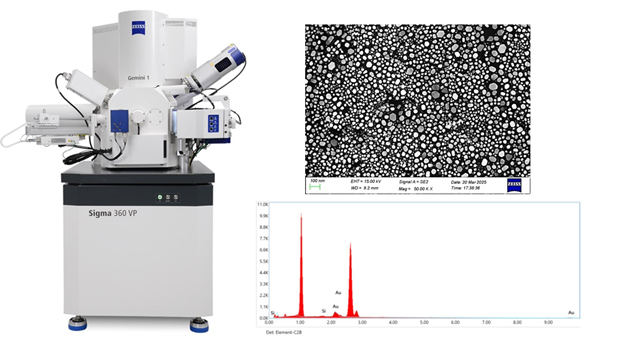
The ZEISS Sigma 360 FE-SEM from ZEISS is a high-performance field emission scanning electron microscope designed for advanced imaging and analytical microscopy across diverse scientific and industrial applications. It delivers exceptional resolution, particularly at low accelerating voltages (down to 1.3 nm at 1 kV and 1.9 nm at 500V), enabling clear imaging of even sensitive or non-conductive samples without requiring conductive coatings, thanks to its variable pressure (VP) mode and NanoVP lite technology. The Sigma 360 utilizes a user-friendly, intuitive 4-step workflow that guides users from setup to image acquisition, making it suitable for both experienced researchers and novice users, and it can be integrated with various detectors (e.g., In-lens SE, ETSE, VPSE, BSE, aSTEM, EDS) to provide comprehensive topographical, compositional, and even crystallographic information. Its versatility makes it an ideal choice for core imaging facilities, supporting research in materials science, nanotechnology, semiconductor development, biological imaging, and failure analysis, among others.
Sigma 360 FE-SEM
High resolution Schottky-FESEM with patented GEMINI-electron optics comprises combined electromagnetic/electrostatic objective lenses and a crossover-free beam path.
Resolution: 0.9 nm @ 15 kV, 1.3 nm @ 1kV
Acceleration voltage: 0.02 kV to 30kV.
Probe current: 3pA - 20nA; with optional high current mode (100 nA)
Detectors:
Stage: 5-axes motorized Cartesian specimen stage with simulated eucentric movement X, Y = 125 mm, Z: 50mm, T= -10° to + 90°, R = 360° continuous,
Magnification: 10 – 1,000,000x
EDS
SmartEDX EDS Analysis System, fixed position, 30mm², 129eV, 600kcps, Silicon Nitride Window
Line as well as area scan is possible.
Sputter Coater
Quorum Q150R-ES Plus Medium range sputter coater & carbon evaporator.
The instrument booking will be done via the Google form. The payment of charges as per the rate chart should be made in advance via SBCollect of SBI. A print copy of the FE-SEM/EDX Requisition Form with the sign of the Head/Supervisor/Guide should be produced at the time of measurements.
Form for Submission of Requisition

